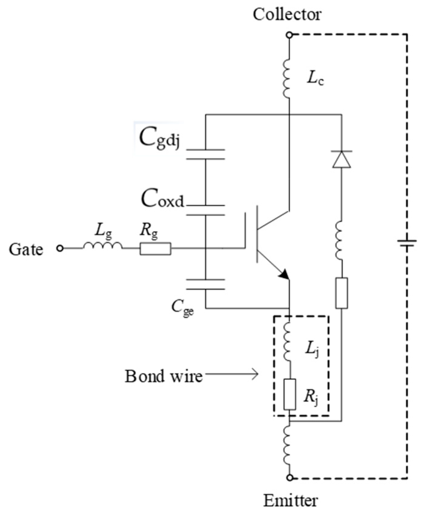
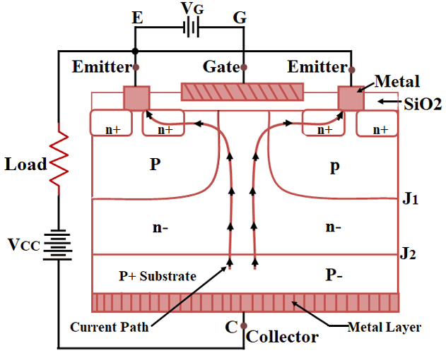
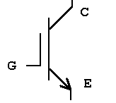
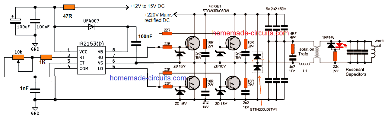
Circuit diagram of an igbt the jfet transistor signifies the construction of current bn any two adjacent igbt cells. A circuit symbol for the igbt is shown below that consists of three terminals namely emitter gate and collectorswitching behavior of igbt.
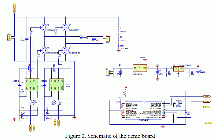
Induction Heater Circuit Using Igbt Tested Homemade
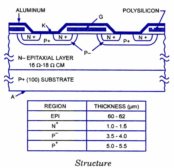
Igbt wiring diagram. Igbt is a short form of insulated gate bipolar transistor combination of bipolar junction transistor bjt and metal oxide field effect transistor mos fet. This is one of several structures possible for this device. In operation the epitaxial region is conductivity modulated by excess holes and electrons. Higginbotham you will be capable to finish. Inverterswagatam homemade inverter circuit diagram intended with inverter welder schematic circuit diagram image size 600 x 600 px and to view image details please click the image. Here is a picture gallery about inverter welder schematic circuit diagram complete with the description of the image please find the image you need.
Its is a semiconductor device used for switching related applications. Ronk phase converter wiring diagram schematics wiring diagram rotary phase converter wiring diagram letters n and u in igbt 3 phase circuit diagram. It allows the mosfet and supports most of the voltage. The basic schematic of a typical n channel igbt based upon the dmos process is shown in figure 1. Introduction to igbt insulated gate bipolar transistors. It is evident that the silicon cross section of an igbt is almost identical to that of a vertical power mosfet except for the pinjecting layer.
Insulated gate bipolar transistor igbt is a new high conductance mos gate controlled power switchthe fabrication process is similar to that of an n channel power mosfet but employs an n epitaxial layer grown on a p substrate. May 30 2020 wiring diagram by anna r.
Gallery of Igbt Wiring Diagram