Generally the pnp transistor can replace npn transistors in most electronic circuits the only difference is the polarities of the voltages and the directions of the current flow. The following is a wiring diagram of an open collector pnp sensor.

Pnp Transistor Circuit Diagram And Working Principle
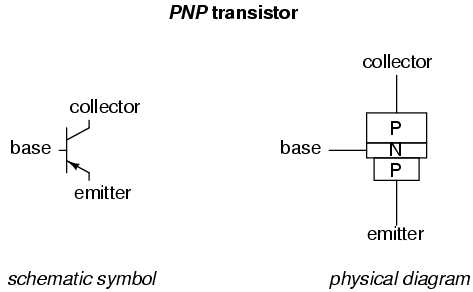
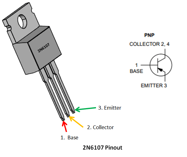
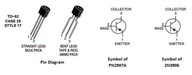
Pnp transistor wiring diagram. A schematic diagram of the pnp transistor is given below. Going from a back view the first lead is the emitter the second lead is the base and the third lead is the collector. Zener voltage regulator circuit this is one of the two configurations of overvoltage protection circuits using zener diode. When connecting to the plc the plc input acts as the load. The pnp transistor like almost all transistors is a 3 lead device. Pnp switched positive npn switched negative switched refers to which side of the controlled load relay small indicator plc input is being switched electrically.
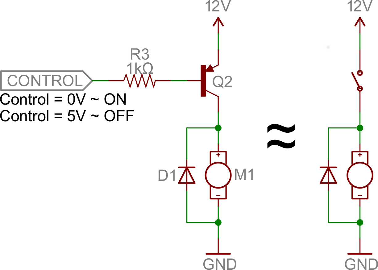
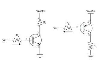
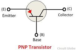
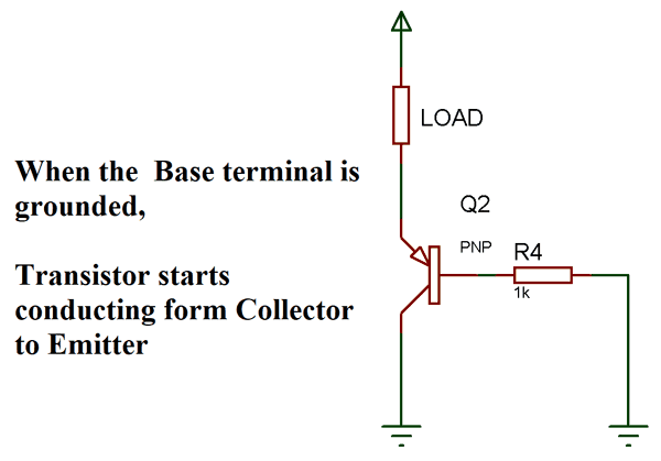
The arrow is sharply pointing towards the base indicating the flow of current from the emitter terminal to the base. Either the load is connected to negative and the positive is switched pnp continue reading an easy way to remember pnp and npn sensor. You will notice that the load appears between the 0v blue and switching wire black. Pnp transistors can also be used as switching devices and an example of a pnp transistor switch is shown below. Symbol of p n p transistor. We will use the most widely used pnp transistor for our circuit the 2n3906.
Heres a simple way remember how to wire up a 3 wire dc pnp or npn sensor. The pinout for a fmmt718 is given in a tabular form below. The 0v blue will be attached to the common input and the switching wire black will be attached to the input number. Pnp transistor symbol the symbol of p n p consists of three terminals emitter base and the collector.
Gallery of Pnp Transistor Wiring Diagram